

EE 236: Electronic Devices Lab
PN junctions, MOSFETs, BJTs and optoelectronic devices - characterisation, circuit implementation and applications.
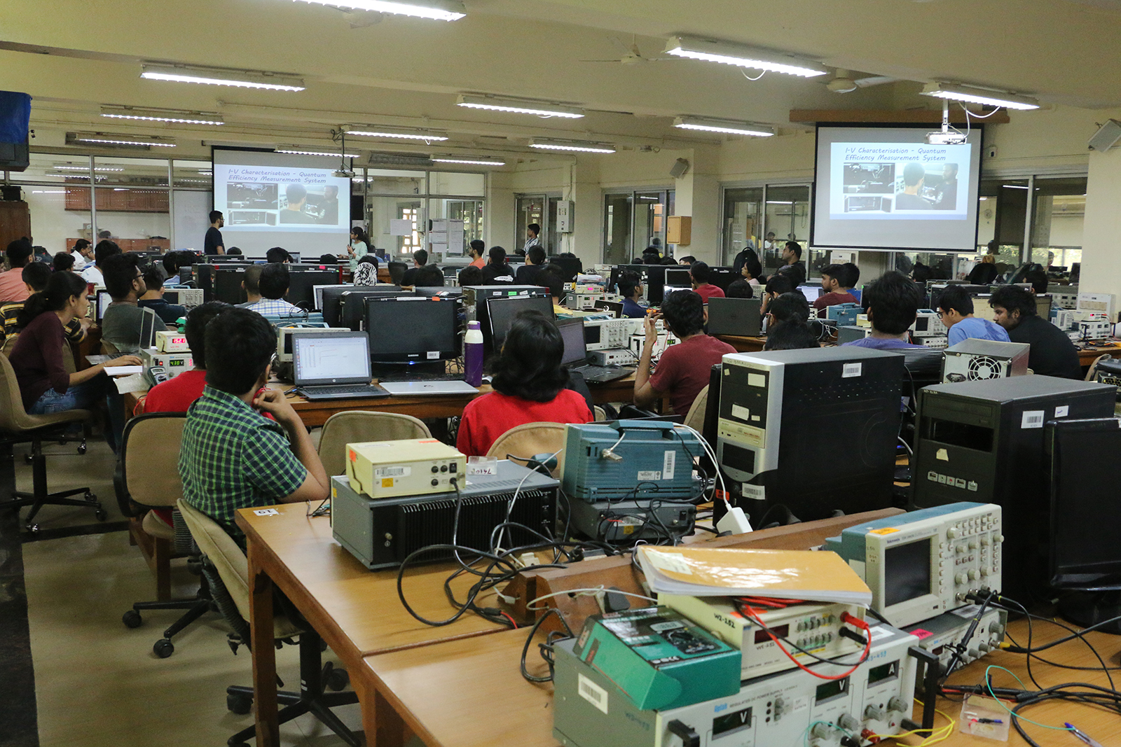
The Electronic Devices Laboratory (EE 236) is a course designed to help students understand the fundamentals of semiconductor devices and their applications. It covers key concepts such as PN junctions, MOSFETs, BJTs, and optoelectronic devices, with experiments focusing on device characterization, circuit implementation, and real-world applications.
Students work with oscilloscopes, signal generators, and specialized testing equipment to analyze device behaviour under different conditions.
Teaching
Course instructors

Schedule
Practical lab experiments schedule, Autumn 2026
| Lab No. | Experiment | Week | Material |
|---|---|---|---|
| Lab 0 | Course introduction slide internal · Course outline slide internal | 28 July – 3 August | Lab 0 handout internal |
| Lab 1 | Introduction to solid state lighting internal | 4 – 10 August | Pre-lab 1 exercise internal · Lab 1 material internal |
| Lab 2 | Introduction to PIN diode and its application internal | 11 – 17 August | Lab 2 handout internal |
| Lab 3 | Introduction to photodiodes and applications internal | 18 – 24 August | Lab 3 handout internal |
| Lab 4 | Introduction to Schottky diode internal | 25 – 31 August | Lab 4 handout internal |
| Lab 5 | Introduction to solar cell internal | 1 – 7 September | Pre-lab simulation internal · Lab 5 handout internal |
| Lab 6 | Lab 6 submission | 8 – 14 September | — |
| — | Mid-semester | 15 – 21 September | — |
| Lab 7 | Introduction to BJT and HBT internal | 22 – 28 September | Lab 7 handout internal |
| Lab 8 | Introduction to NMOS, PMOS, CMOS and MOSCAP internal | 29 September – 5 October | Lab 8 handout internal |
Course resources
Material and links
Every handout, pre-lab exercise and slide deck for this course is linked from the schedule below.